Power Electronics
Class-D Half-Bridge Resonant Converter
ODE validation, FHA accuracy limits, and ZVS design — groundwork for RL-based parameter tuning of DBD drives
1Overview
The Class-D half-bridge with a series-resonant tank is the workhorse topology for high-frequency AC loads such as Dielectric Barrier Discharge (DBD) plasma reactors. Conventional design relies on the First-Harmonic Approximation (FHA) — a linearization that treats the square-wave output as a sinusoid at the fundamental frequency. FHA gives closed-form design equations but breaks down away from resonance and entirely for nonlinear loads.
This work has two objectives: (1) validate a full nonlinear ODE model against the FHA baseline, and (2) characterize the ZVS–power trade-off using the ODE, identifying where conventional analytical design fails and motivating an RL-based approach.
ODE vs FHA at resonance: 0.18% error — ODE correctly implemented
ZVS onset: fsw/f0 ≈ 1.05
Power penalty at 1.1f0: ~8%
FHA error at 0.5f0: 46% — harmonics dominate
2Circuit Model
The half-bridge produces a square wave switching between 0 and Vdc at frequency fsw. This drives a series resonant tank (Lr, Cr) into a load R. In the soft-switching model, a midpoint capacitance Co (MOSFET output capacitance) is added in parallel with the lower switch.
  V_dc ─── S1 ──┬── L_r ── C_r ── R ──┐
                │                      │
               C_o  v_mid              │
                │                      │
   0V  ─── S2 ──┴──────────────────────┘
The two state variables during conduction are the inductor current iL and capacitor voltage vC:
diL/dt = (vin(t) − vC − iL·R) / Lr
dvC/dt = iL / Cr
During dead time, vmid becomes a free variable and the system becomes 3rd order — Co charges or discharges driven entirely by iL.
| Parameter | Value | Unit |
|---|---|---|
| Vdc | 400 | V |
| Lr | 50 | μH |
| Cr | 100 | nF |
| R | 10 | Ω |
| Co | 500 | pF |
| f0 | 71.18 | kHz |
| Q = ω0Lr/R | 2.24 | — |
3FHA Baseline
The half-bridge square wave has a Fourier fundamental amplitude of V1 = 2Vdc/π. The DC component is blocked by Cr. Retaining only the fundamental, the voltage transfer function is:
H(jω) = R / [R + j(ωLr − 1/ωCr)]
|H| = R / √[R² + (ωLr − 1/ωCr)²]
At resonance ωsw = ω0 = 1/√(LrCr), the reactive terms cancel (Z = R), giving peak current Ipeak = 2Vdc/(πR) = 25.46 A and peak load voltage VR = 254.65 V.
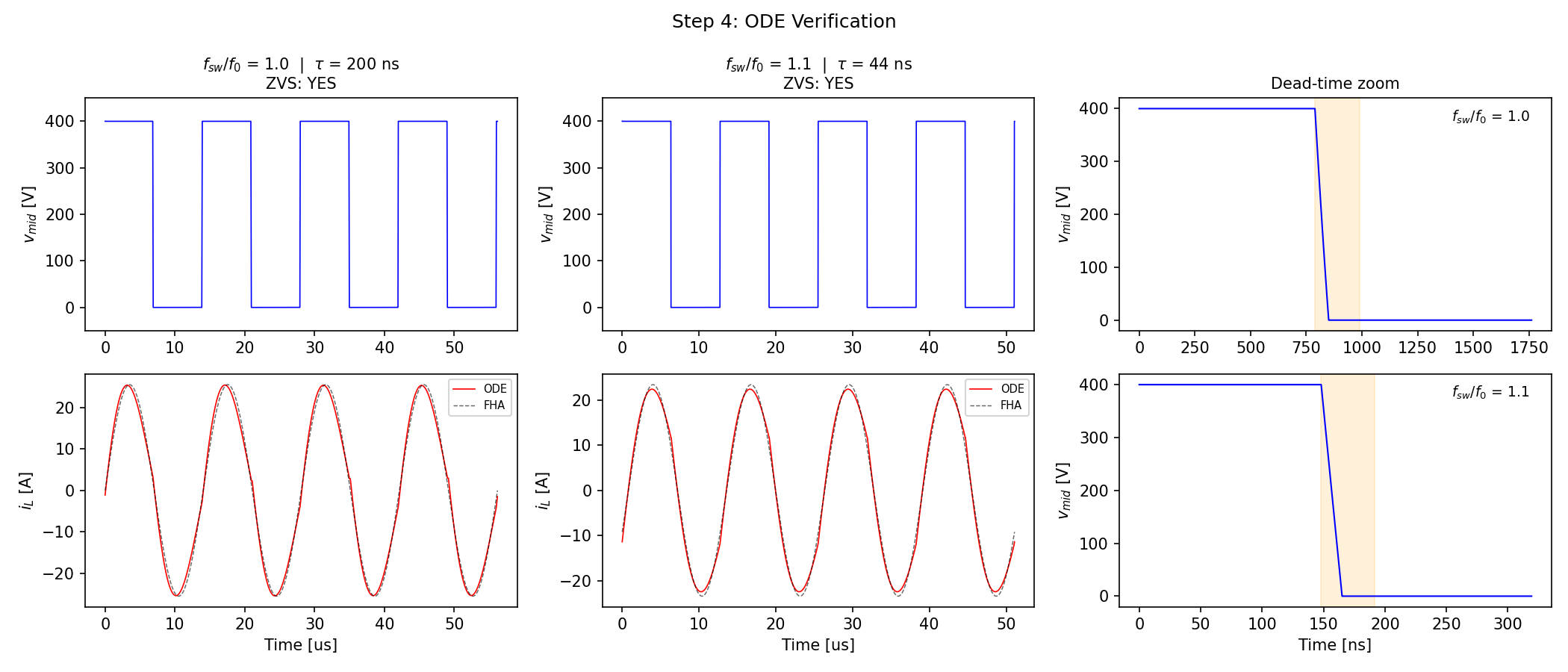
4ODE Validation
The ODE is integrated with scipy's Radau solver (max step Tsw/200) for 80 cycles to reach steady state. At resonance, the ODE matches the FHA to within 0.18% for both peak current and peak voltage — confirming correct implementation and sufficient solver accuracy.
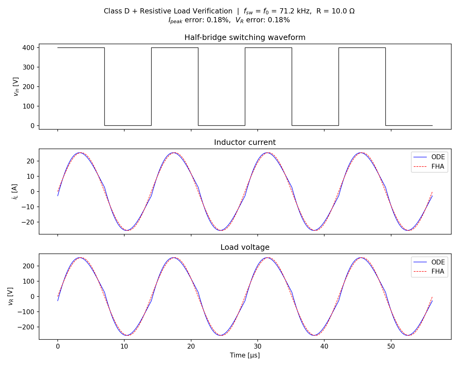
| Quantity | FHA | ODE | Error |
|---|---|---|---|
| Ipeak | 25.46 A | 25.42 A | 0.18% |
| VR,peak | 254.65 V | 254.19 V | 0.18% |
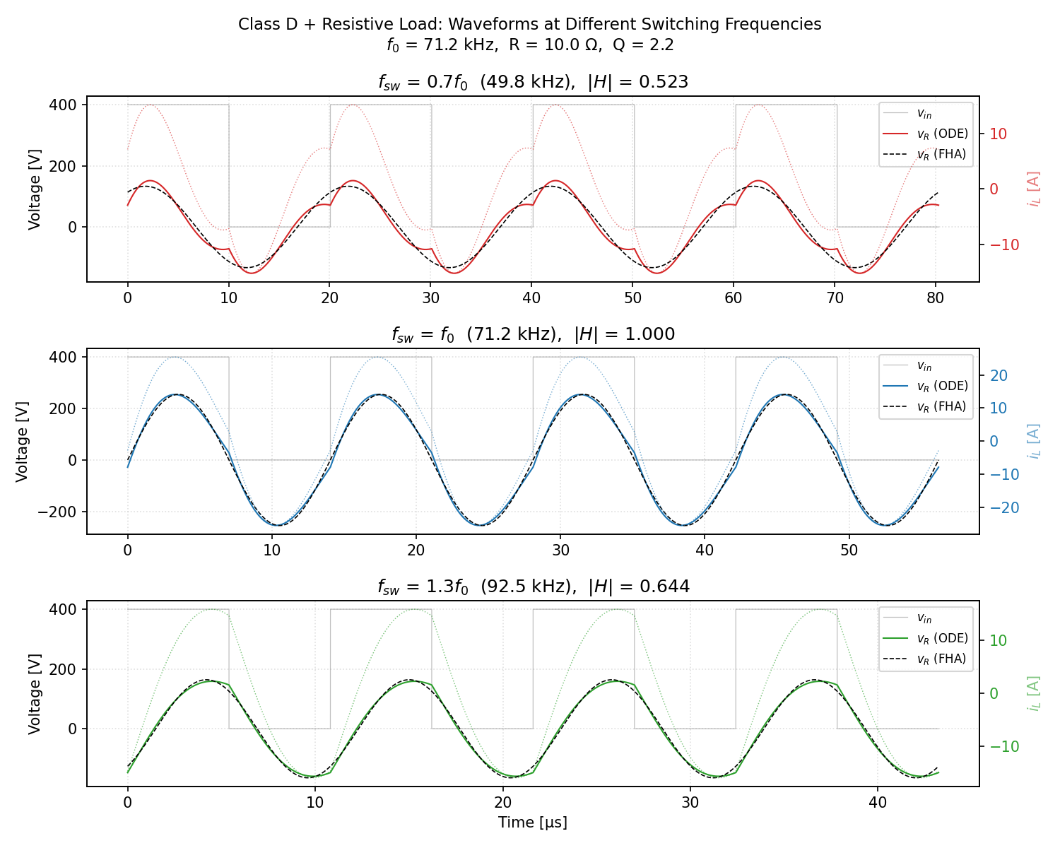
5Bode Plot & Frequency Sweep
The FHA transfer function is compared against ODE-extracted gain and phase across a 4:1 frequency range. Near resonance (0.85 ≤ fsw/f0 ≤ 1.15) agreement is within a few percent. At low frequencies the error grows sharply — at 0.5f0, the third harmonic lands near the resonant peak and is amplified, which the FHA cannot capture.
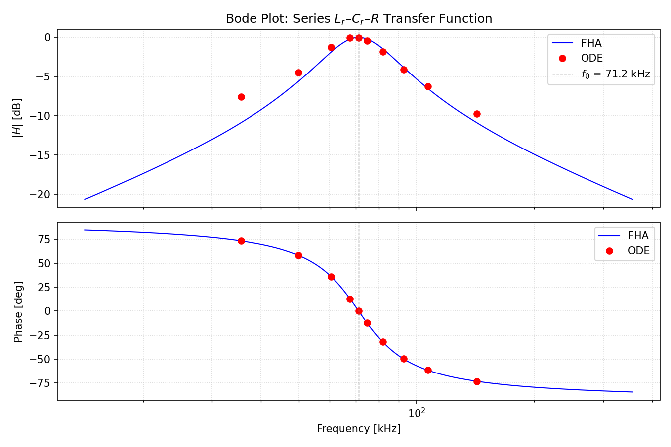
| fsw/f0 | fsw [kHz] | |H| FHA | |H| ODE | Error |
|---|---|---|---|---|
| 0.50 | 35.59 | 0.286 | 0.418 | 46.3% |
| 0.70 | 49.82 | 0.523 | 0.596 | 13.9% |
| 0.85 | 60.50 | 0.808 | 0.868 | 7.4% |
| 0.95 | 67.62 | 0.975 | 0.998 | 2.4% |
| 1.00 | 71.18 | 1.000 | 0.998 | 0.2% |
| 1.05 | 74.74 | 0.977 | 0.954 | 2.4% |
| 1.15 | 81.85 | 0.847 | 0.809 | 4.5% |
| 1.30 | 92.53 | 0.644 | 0.624 | 3.1% |
| 1.50 | 106.76 | 0.473 | 0.488 | 3.3% |
| 2.00 | 142.35 | 0.286 | 0.327 | 14.4% |
6ZVS & Dead-Time Design
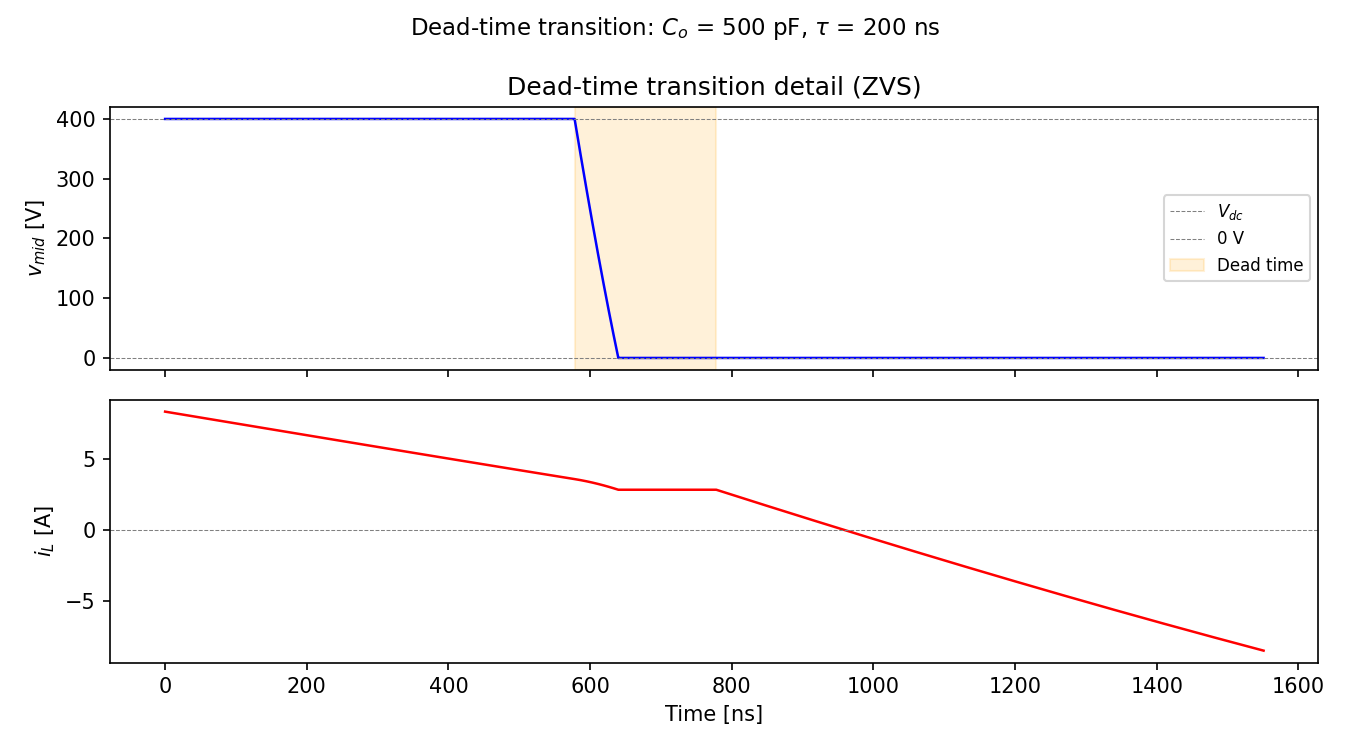
ZVS requires iL > 0 at the switching instant so that Co can discharge from Vdc to zero before the incoming switch turns on. The FHA gives the current at the half-period and the minimum required dead time:
iL(T/2) = −(V1/|Z|) · sin φI
τmin = Co · Vdc / |iL(T/2)|
At resonance φI = 0, so iL(T/2) = 0 and τmin → ∞ — ZVS is impossible without operating above resonance where the tank becomes inductive.
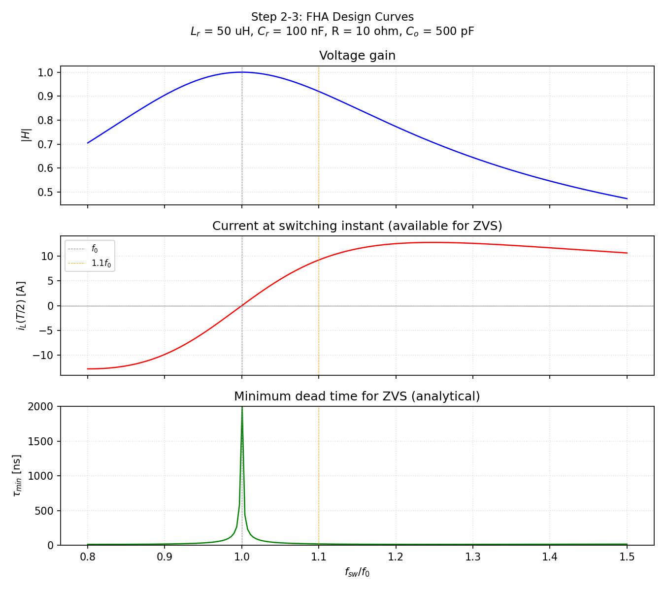
| fsw = f0 | fsw = 1.1f0 | |
|---|---|---|
| |H| | 1.000 | 0.920 |
| Ipeak | 25.46 A | 23.42 A |
| φI | 0° | −23.1° |
| iL(T/2) | 0 A | 9.19 A |
| τmin | ∞ | 21.8 ns |
| Pload | 3242 W | 2743 W |
7Design Trade-off
A sweep of fsw/f0 from 0.9 to 1.3 quantifies the fundamental ZVS–power trade-off. The ODE measures actual vmid at the end of dead time and actual delivered power, revealing where the FHA current estimate is optimistic vs. pessimistic.
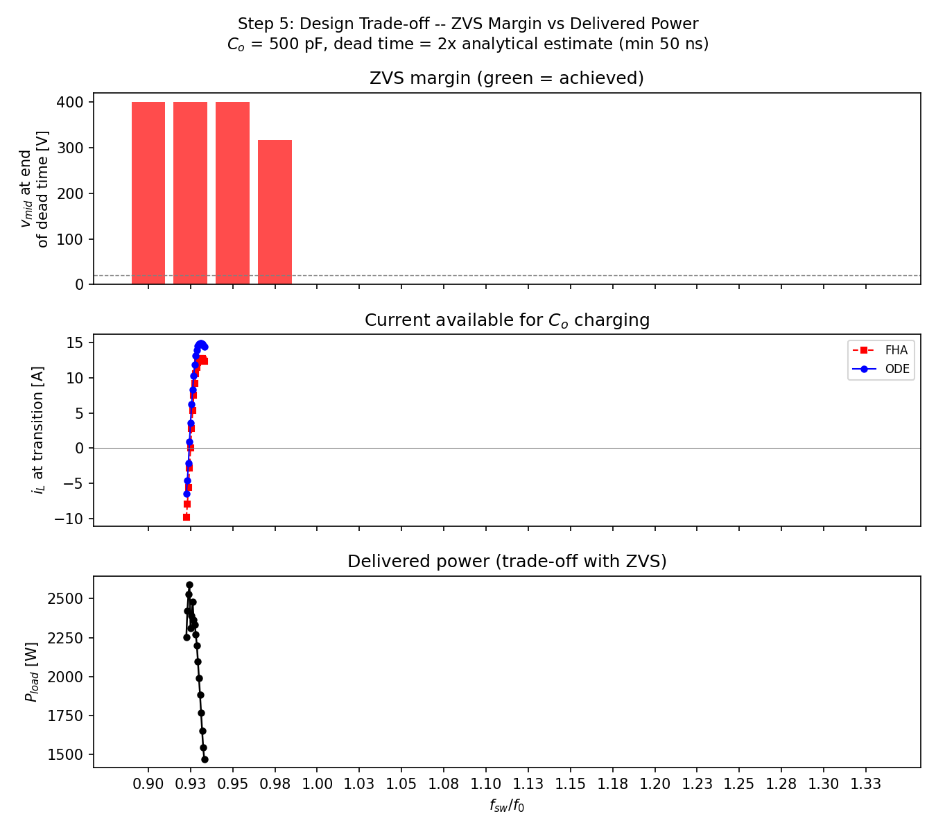
ZVS onset: fsw/f0 ≈ 1.05
Power penalty: ~8% at 1.1f0, ~20% at 1.2f0
FHA accuracy: underestimates ZVS current below resonance (harmonics help); overestimates above — ODE verification required
8Conclusions
The conventional FHA-based design pipeline is accurate only near resonance with linear loads, and fails in two key ways:
- Harmonic content: At fsw < 0.85f0, higher harmonics are amplified by the tank — FHA underestimates current by up to 46%. The ODE captures this correctly.
- Nonlinear loads: For DBD loads where impedance alternates between capacitive and resistive within each cycle, FHA linearization fails entirely.
This validated ODE forms the simulation environment for an RL agent tasked with jointly optimizing (Lr, Cr, τ, fsw) for a DBD load — replacing the iterative manual design loop with a single learned policy.